Introduction
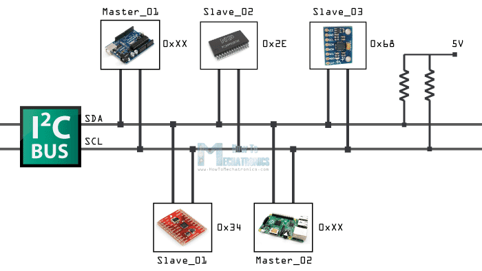
The I2C communication bus is very popular and broadly used by many electronic devices because it can be easily implemented in many electronic designs which require communication between a master and multiple slave devices or even multiple master devices. The easy implementations come with the fact that only two wires are required for communication between up to almost 128 (112) devices when using 7 bits addressing and up to almost 1024 (1008) devices when using 10 bits addressing.
How It Works
How is it possible, to communicate between so many devices with just two wires? Well, each device has a preset ID or a unique device address to the master can choose with which devices will be communicating.
The two wires or lines are called Serial Clock (or SCL) and Serial Data (or SDA). The SCL line is the clock signal which synchronizes the data transfer between the devices on the I2C bus and it’s generated by the master device. The other line is the SDA line which carries the data.
The two lines are “open-drain” which means that pull-up resistors need to be attached to them so that the lines are high because the devices on the I2C bus are active low. Commonly used values for the resistors are from 2K for higher speeds at about 400 kbps, to 10K for lower speeds at about 100 kbps.
I2C Protocol
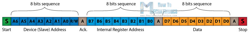
The data signal is transferred in sequences of 8 bits. So after a special start condition occurs comes the first 8 bits sequence which indicates the address of the slave to which the data is being sent. After each 8 bits sequence follows a bit called Acknowledge. After the first Acknowledge bit in most cases comes another addressing sequence but this time for the internal registers of the slave device. After the addressing sequences follow the data sequences as many until the data is completely sent and it ends with a special stop condition.
Let’s take an even closer look at these events. The start condition occurs when data line drops low while the clock line is still high. After this, the clock starts and each data bit is transferred during each clock pulse.
The device addressing sequence stars with the most significant bit (MSB) first and ends with the least significant bit (LSB) and it’s actually composed of 7 bits because the 8th bit is used for indicating whether the master will write to the slave (logic low) or read from it (logic high).
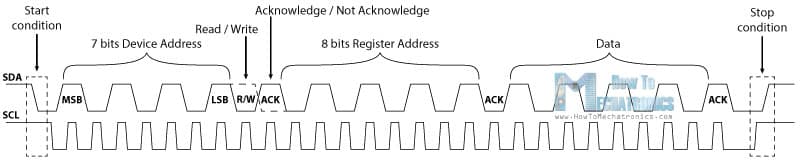
The next bit AKC/ NACK is used by the slave device to indicate whether it has successfully received the previous sequence of bits. So at this time, the master device hands the control of the SDA line over to the slave device and if the slave device has successfully received the previous sequence it will pull the SDA line down to the condition called Acknowledge. If the slave does not pull the SDA line down, the condition is called Not Acknowledge and means that it didn’t successfully receive the previous sequence which can be caused by several reasons. For example, the slave might be busy, might not understand the received data or command, cannot receive any more data and so on. In such a case the master device decides how it will proceed.

Next, is the address of the internal register. The internal registers are locations in the slave’s memory containing various information or data. For example, the ADX345 Accelerometer has a unique device address and additional internal register addresses for the X, Y, and Z axis. So if we want to read the data of the X-axis, first we need to send the device address and then the particular internal register address for the X-axis. These addresses can be found in the datasheet of the sensor.